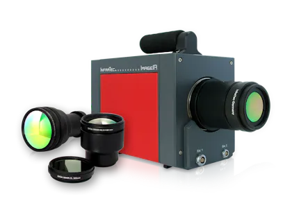
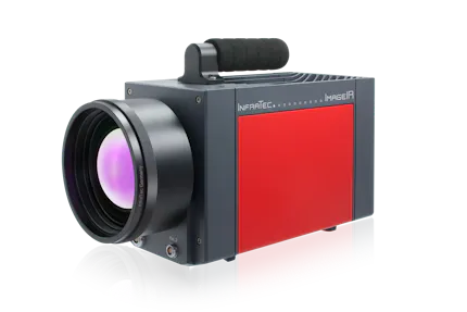
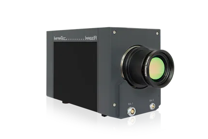
Electronic / Semiconductor Testing Solution - E-LIT
Modular Automated Test Bench
2D and 3D analysis of electronic and semiconductor devices
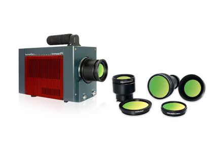
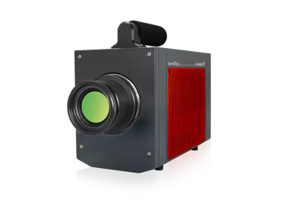
Modular test bench with a radiometrically calibrated infrared camera for precise lock-in measurements
Highly sensitive temperature measurement and reliable detection of thermal anomalies in the mK and μK range
Spatial location of point and line shunts, oxide defects, transistor and diode failures in multilayer PCBs and multi-chip modules
Detection of “watermarks” and thermal signatures for authenticity verification of microchips
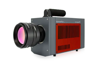
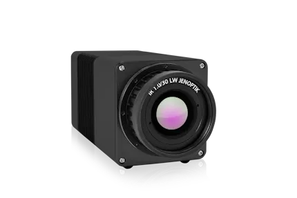
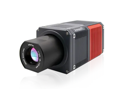
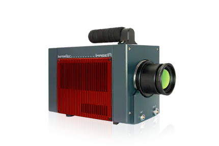
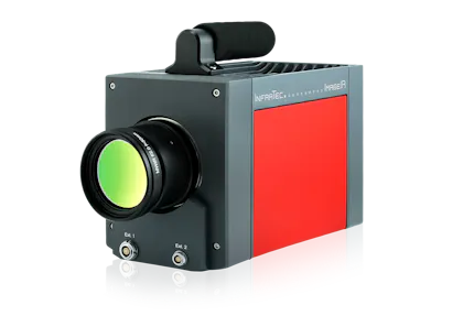
Designed for use with thermographic systems with cooled and uncooled detectors
Native resolutions of up to (2,560 × 2,048) IR pixels and multiples of that through stitching
Maximum flexibility due to the lens turret
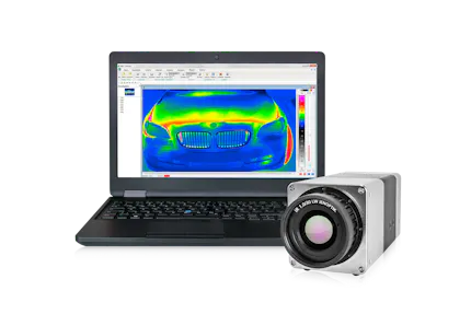
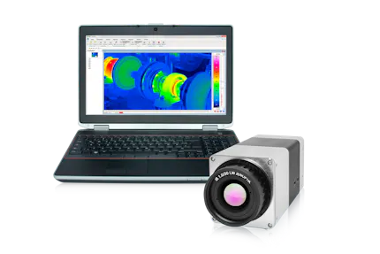
IRBIS® 3 active thermographic software with a wide range of analysis options


Automated Lock-In measurement with E-LIT from InfraTec


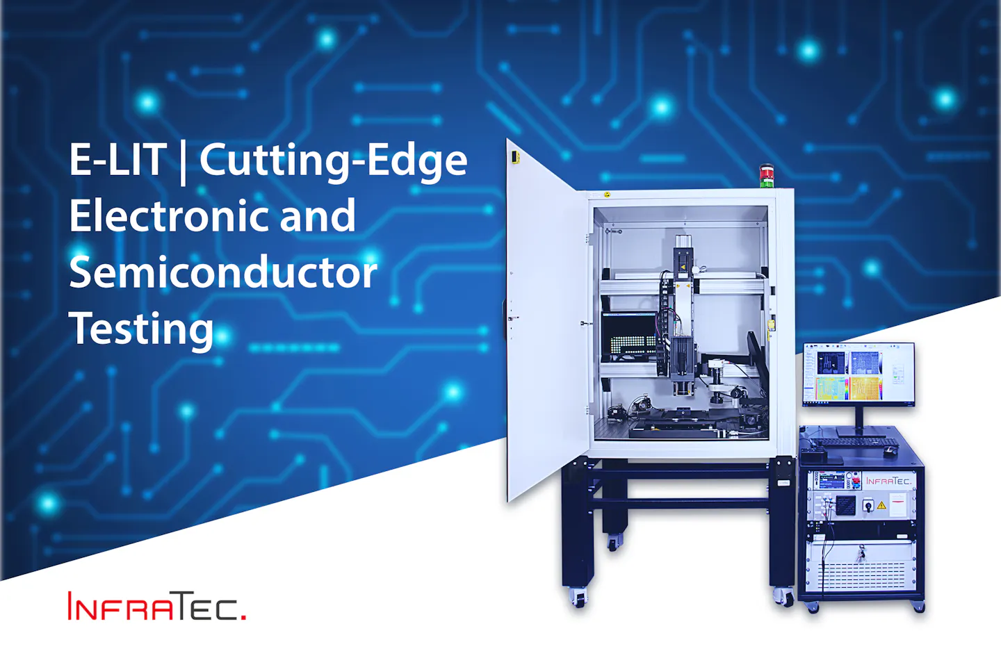


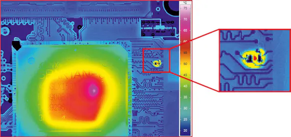
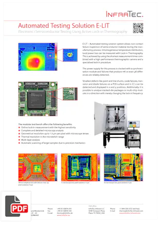
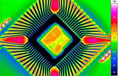
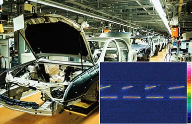
E-LIT – Lock-In Thermography for electronics is an automated testing system used in non-destructive testing (NDT) It enables contactless failure analysis as well as the verification of the authenticity of semiconductor materials, electronic components, and electronic circuits. Inhomogeneous temperature distributions and local power losses can be detected using lock-in Thermography and a high-performance, radiometrically calibrated infrared camera.
The source-measure units (SMUs, also known as SourceMeters) used to precisely supply power to the component under test can be configured directly through the E-LIT system. Even faults that cause temperature deviations of only mK or μK can be detected.
Even the smallest defects in components and assemblies, such as integrated circuits, can be precisely located and visualized. These include:
Point and line short circuits,
Oxidation, transistor, and diode defects,
Resistive opens,
Leakage currents,
ESD defects, and
Latch-up effects.
By changing the lock-in frequency, defects in stacked-die packages or multi-chip modules (3D packaging, advanced packaging) can also be spatially localized (depth measurement). In combination with algorithm-based pattern recognition, it is also possible to detect, for example, circuit tampering.
The powerful Lock-in thermography software uses algorithms and routines from the latest scientific publications for these and similar tasks.
To resolve the smallest geometric structures, the E-LIT test bench uses high-performance microscope objectives and SIL lenses. When high-resolution detectors with up to (2,560 x 2,048) IR pixels are used, even microscopic defects can be detected and characterized.
The automated E-LIT test bench is of interest to developers and manufacturers of
Microchips, PCBs, electronic assemblies,
Servers,
Power semiconductors,
Solar and PV modules,
High-frequency components and
Optoelectronic components.
Electronics and Semiconductor Module Testing by means of Lock-in Thermography
Find out in our white paper how you can use lock-in thermography to detect faults in electronic and semiconductor components. Benefit from our practical tips and achieve the best possible measurement results with the E-LIT test bench from InfraTec.


Benefits of the Modular Test Bench
Measurement using a test bench: failure analysis of circuits—from the printed circuit board (PCB) up to the smallest detail
Customized modular measuring station, e. g. with X-Y table and Z-axis manually or motorized adjustable, for precise positioning and individual adjustment of the working distances depending on the size of the measured object, for example chips, modules, wafers and wafer samples, printed circuit board assemblies, as well as solar cells, micromechanics, thin-film electronics, hybrid and high-frequency circuits
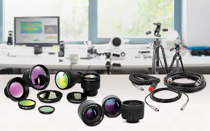
Flexibility through variable components, e.g. different lenses, mounting fixture for the measured object or contact options – even greater flexibility through the use of a lens turret
Real-time lock-in measurement on circuit boards with maximum sensitivity, without delayering or deprocessing the component, and without removing chips or assemblies or “unpackaging” the IC component
Complete and detailed microscopy analysis
Geometrical resolution up to 1.3 μm per pixel with microscope lenses
Thermal resolution in the microkelvin range
High-voltage test bench with interlocked contact protection against accidental contact and an operating status indicator light
Integration of a high-voltage source meter unit up to 3kV
Integrated IV curve tracer for i-v characterization
Multi-layer chip testing
Automatic scanning of larger samples due to precision mechanics


For electronics testing, methods such as Scanning Acoustic Microscopy (SAM), 2D or 3D X-ray imaging, Emission Microscopy (EMMI) or Photon Emission Microscopy (PEM), Liquid Crystal Thermography (LCT), Thermally Induced Voltage Alteration (TIVA / SEI), Magnetic Current Imaging (MCI) / SQUID microscopy, or Optical Beam Induced Resistance Change (OBIRCH) can be employed either as alternatives to or in addition to lock-in thermography, depending on the specific issue under investigation.
SAM, for example, is very effective for interfaces, delaminations, and acoustic impedance jumps, but requires the use of a coupling fluid. 2D and 3D X-ray imaging is ideal for identifying density, geometric, and material contrasts. Defects without sufficient X-ray contrast or with unclear functional relevance are often difficult to evaluate. In the OBIRCH method, a laser heats the sample locally, and the resulting changes in resistance or current are measured. To do this, the object under analysis often must be decapsulated. Furthermore, heating with the laser can lead to damage to sensitive structures.
Lock-in Thermography is recommended whenever a quick, noncontact, and comprehensive test is required and the defects being sought affect the heat flow or the electrical/thermal function of the component. Another key benefit of lock-in thermography is that it is a non-destructive testing method: Subsequent analyses using other measurement methods can be carried out without any issues to obtain additional results.
Thermographic Software IRBIS® 3 active for semiconductor testing
Operational software with comprehensive analysis options in laboratory conditions
Software add-on for automatic failure classification based on parameter settings
Intuitive user interface for easy operation
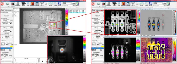
Real-time display of the electronic object being measured in various states
A wide range of storage options for image data, measurement results, and measurement configurations (e.g., ROIs and analysis workflows) Visualization of complex intensity information with a freely selectable phase angle
Merging live and amplitude image
Optional: IV measurement, under sampling, drift compensation, DC-mode, power loss measurement, user and protocol administration, interface preparation: e.g. Profibus, Ethernet


Quick Lens Changes with Maximum Positioning Accuracy
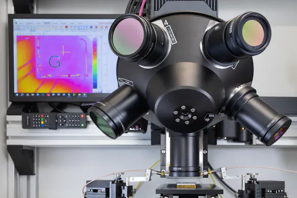
InfraTec's compact lens turret expands the capabilities of the E-LIT automated electronics test system and facilitates the precise detection of even the smallest defects on printed circuit boards and within circuits.
A "region of interest" identified once by the user remains in place even if the field of view changes after a lens change, eliminating the need for time-consuming repositioning. At the same time, vibrations and unintended heat input are minimized.
Up to five microscope lenses with different magnifications can be mounted on the lens turret, enabling details as small as a few µm to be resolved. Motorized lens changes take only a few seconds. The IRBIS® software provides convenient control of lens selection, camera focusing, and sample positioning. Saved focus parameters and a programming interface support automated measurement sequences.
The compact design with an angled axis of rotation is advantageous for contacting the sample in the E-LIT test station. The lens turret is also suitable for other space-saving laboratory setups.


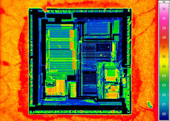
Detection and allocation of faults in the µK range


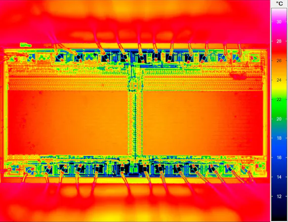

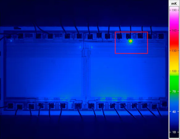


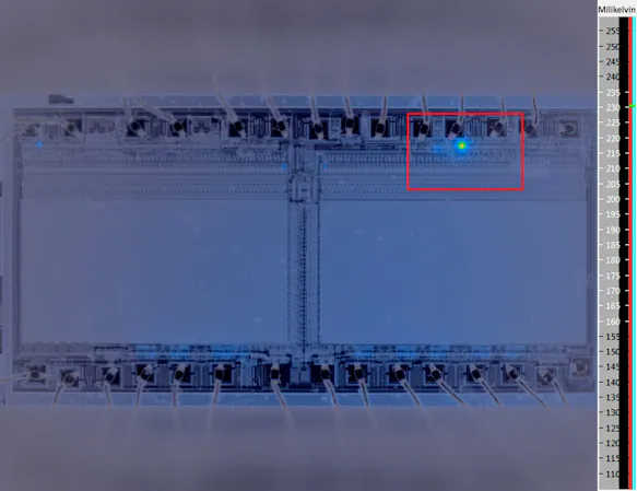
Thermographic Images with Different Optics
Telephoto Lens 100 mm


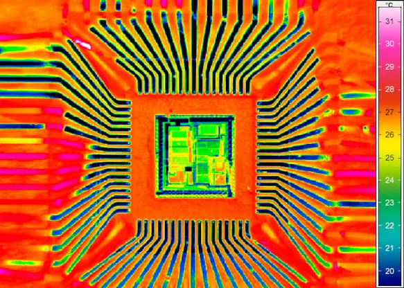
Microscopic Lens 3×

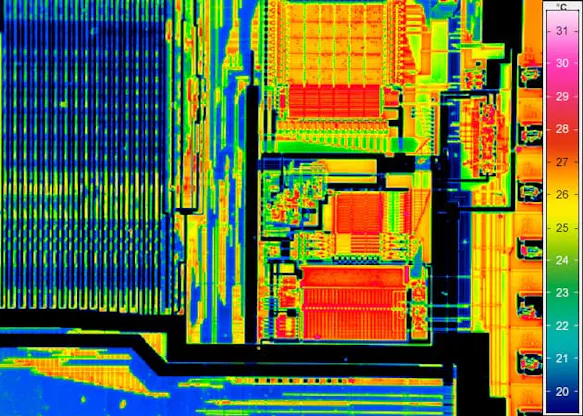
Microscopic Lens 1×



Would You Like to Know More?
It is not unusual for tasks to be associated with special requirements. Discuss your specific application needs with our specialists, receive further technical information or learn more about our additional services.




Product Flyer
Get all the information you need at a glance in our product flyers